

Applets
contents
visual index
 introduction std_logic_1164 gatelevel circuits delay models flipflops adders and arithm... counters LFSR and selftest memories programmable logic state-machine editor misc. demos I/O and displays DCF-77 clock relays (switch-le... CMOS circuits (sw... RTLIB logic
 RTLIB registers
 latches registers counter shift-register 16-bit setta... ROM RAM DPRAM stack stack address-decoder byte- vs. wo... memory demo ALU (user-de... PIO 8255 PIO 8255 USART 8251 8251 text-to... 8251 transmi... 8251 databit... 8251 parity ... 8251 prescaler 8251 loopbac... 8251 loopbac... 8251 error d... microprogram full micropr... 1-address da... 3-address da... 2-address da... Prima processor D*CORE MicroJava Pic16 cosimulation Mips R3000 cosimu... Intel MCS4 (i4004) image processing ... [Sch04] Codeumsetzer [Sch04] Addierer [Sch04] Flipflops [Sch04] Schaltwerke [Sch04] RALU, Min... [Fer05] State-Mac... [Fer05] PIC16F84/... [Fer05] Miscellan... [Fer05] Femtojava FreeTTS
The RS-232 protocol for serial data communication is rather simple. For a thorough explanation, see the RS-232 article on Wikipedia. The transmitter is connected to the receiver via just two wires (signal and ground) for unidirectional communication. For bidirectional communication between two devices, two separate unidirectional channels are combined, with the transmitter of one device connected to the receiver of the other device. In this case, two signal wires and a common ground connection are required. Several variants of the protocol are in use, which differ in the actual symbol encoding via voltage levels or currents. The original current-loop encoding used a steady-state current of 20 mA to indicate a passive line and zero amps to indicate an active state. This way, a broken connection between the transmitter and receiver could be detected immediately. In microprocessor systems, it is often more convenient to encode the symbols with voltages. Here, a high level ('1') is used to indicate an inactive line, while a low level ('0') indicates the active state of the line. Often, extra converter chips like the popular MAX-232 driver are used to amplify the output signal of a weak transmitter chip and to protect a microprocessor system from glitches on the external communication line(s).
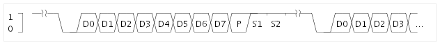
To indicate the beginning of a data transmission, the transmitter first drives the signal line to the low (active) state for one period of the transmitter clock. This is called the start bit. During the next periods of the transmitter clock, the selected number of data bits (usually five to eight) are transmitted starting with the least significant bit. If enabled, a parity bit is inserted after the most significant data bit. Finally, the signal line is kept high (passive) for at least one transmitter clock period; this is called the stop-bit. Often, two-stop bits are used. After the stop bit(s), the signal line is kept in the idle (inactive) state until the start bit of the next data is to be transmitted. The example figure below shows the transmission with one startbit, eight databits, parity bit, and two stopbits. Obviously, the receiver must be configured to use the same number of data-bits, parity, and stop-bits as the transmitter. Also, the bit clock of the receiver must match the transmitter's clock within a few percent for successful data reception:
The simulation model used in this applet is based on the Intel 8251 chip, which was originally developed for systems based on the 8080/8085 series 8-bit microprocessors, but can also be attached to the system buses of other microprocessor systems. The original 8251 chip supports both asynchronous and synchronous serial communication, but the Hades simulation model as yet only supports the more common asynchronous mode, where the serial communication line is kept idle between transmissions. The operation of the chip and its several operating modes will be explained below and in the following applets.
The schematics shows the 8251 chip in the center, with the bus-interface signals on the left and the signals of the serial-communication interface on the right. The serial communication signals can be subdivided into three main groups:
- Shown at the top are the transmitter output TXD and two transmitter status outputs, the transmitter ready signal TXRDY and the transmitter empty signal TXE (sometimes also called TXEMPTY). An external clock generator is required to drive the nTXC clock input to generate the reference bit clock for the transmitter.
- Similarly, the bottom group of signals belongs to the receiver with the RXD data input and a separate nRXC bit clock input. The RXRDY status output signals that the receiver has received an incoming character, which should then be read by the CPU. As the RXRDY, TXRDY, and TXE status signals indicate that data has been received or transmitted, they can also be used to generate interrupt requests to the host microprocessor; some additional logic might be required for this.
- The middle group of signals are the standard flow-control or modem-control lines, namely clear-to-send nCTS, ready-to-send nRTS, data-set-ready nDSR, and data-terminal-ready nDTR. The nCTS signal also directly controls the transmitter block; characters are only transmitted while nCTS is held low.
Applet usage and demonstration sequence
Before the 8251 chip can be used for actual communication, its operating mode must first be selected via writing the corresponding mode and command registers. To avoid the dozens of mouse-clicks of the input switches for the initialization sequence, this applet includes a stimuli-generator that automatically generates the input sequence to enable the 8251 chip for standard RS-232 asynchronous data transmission with the following parameters: 8 data-bits, no parity, and 2 stop-bits. After the initialization sequence has completed, you can use mouse-clicks or the bindkeys to interactively control the data-bus and control signals of the USART to transmit characters via the transmitter output or to read the status register. The transmitter clock is set to a very slow rate of 0.5 Hz, which allows watching the serial communication bit for bit during the interactive simulation.A short introduction about the registers and command set of the 8251 chip is provided at the end of this page; for a full explanation of all features please download and consult the datasheet. The predefined input sequence used by this applet takes about 90 seconds, deliberately slowed down to allow watching all signal changes during the animation. If you prefer to study the signal waveforms after a quick initialization of the 8251, please click here. The input sequence does the following:
- initalize all lines of the 8251 bus-interface to their inactive values.
- generate a reset-pulse to initialize the 8251 chip.
- write the mode-register to select asynchronous communication with 8-databits, no parity, and 2 stopbits.
- write the command-register to enable the transmitter.
- write the data-register to transmit a 0x55 character.
- write the data-register to transmit a 0xAA character.
- write the data-register to transmit a 0x33 character.
- write the data-register to transmit a 0x0F character.
- the bus-interface values are then kept ready for data transmission.
Once this sequence is completed, you can use the DATA-switch to select a new data value for transmission and generate a low-pulse (1-0-1) on the nWR write input to start a new data transmission operation. Please wait until the TXRDY (transmitter ready) status line goes high again before selecting a new DATA input value and a new nWR write pulse. It might be a good idea to add signal probes to the data-bus, transmitter output, and a few control signals, so that you can analyse the timing dependencies after transmitting a few characters. To add a probe, move the mouse to a vertex of the signal in question, then type the 'p' bindkey. If necessary, restart the simulation.
To control the applet, either click the input switches, or type the following bindkeys: 's' for chip-select, 'r' for read-enable (nRD), 'w' for write-enable (nWR), 'd' and 'D' to decrement/increment the DATA bus input. Remember to use click/shift+click/control+click combinations, or use the property-sheet (popup-edit) to control the DATA bus input switch. The switch should be set to the tristate state during read operations (via control+click).
After you have played with the applet to explore the data transmission, please visit the following applets for the next demonstrations of the 8251 chip:
- Introduction with text-to-speech audio
- Basic transmitter setup and usage
- Selection of 5,6,7,8 data-bits
- Demonstration of the parity modes
- Loopback demo of transmitter and receiver
- Receiver error checking
- MIPS-based microprocessor system with 8251 UART
8251 USART description
The Intel 8251 chip integrates a standard (8-bit) microprocessor bus interface, one serial transmitter, and one serial receiver. A few additional control lines are provided for modem-control and efficient handshaking or interrupts.The bus-interface consists of the bidirectional 8-bit data-bus (lines D7..D0) and the read/write control-logic with the following inputs:
  DATA  (D7..D0)    8-bit bidirectional data-bus
  RESET             active-high reset input
  nCS               chip select input (active low)
  CnD               command (high) or data (low) selection input
  nRD               read enable input (active low)
  nWR               write enable input (active low)
The transmitter logic consists of the nTXC transmitter clock input, the TXD data output, and two status output signals called TXE (or TXEMPTY) and TXRDY. The receiver logic consists of a separate RXC receiver clock input, the RXD data input, the RXRDY status output, and one programmable status line called SYNDET/BD. Four additional lines, provide modem-control capabilities. The output lines nDTR (data transmit ready) and nRTS (ready to transmit) can be written by the host microprocessor, while the input lines nCTS (clear to send) and nDSR (data send ready) can be read by the host microprocessor. The nCTS input signal also directly controls the transmitter of the 8251 chip. When nCTS goes high, the transmitter will finish an ongoing data transfer but subsequent transmissions will wait until nCTS becomes low again. If unused, the nCTS input must be tied to ground or the transmitter will be effectively disabled. The Hades symbol groups the bus-interface signals on the left side, the transmitter signals on the upper part of the right side, and the receiver signals on the lower part of the right side. The modem-control signals are placed in the middle of the right side.
Similar to the 8255 chip explained in the previous applets, the bus-interface of the 8251 is asynchronous. The CnD (command/not-data) control input selects between command and data transfers; this signal could also be called an address input A0. The resulting behaviour is the following:
  reset  nCS  nRD  nWR  CnD  data  |  behaviour
 -------------------------------------+-----------------------------------
      1    *    *    *   *      *  |  device reset
      0    1    *    *   *      *  |  device passive
      0    0    1    1   *      *  |  device selected but inactive

      0    0    0    1   1   read  |  read status register
      0    0    1    0   1   write |  write mode/command/sync registers

      0    0    0    1   0   read  |  read receive buffer
      0    0    1    0   0   write |  write transmit buffer

      u    u    u    u   u      *  |  any undefined U,X,Z value will
                                   |  invalidate the simulation model
The chip contains seven user-visible registers, five of which can only be written, and two of which can only be read. These are the following:
  mode register        - sync/async operation mode and parameters
  command register     - enable/disable and error resetting
  sync 1 character     - 8-bit dataword (sync mode only)
  sync 2 character     - 8-bit dataword (sync mode only)

  transmit buffer      - 8-bit register for outgoing data
  receive buffer       - 8-bit register with incoming data
  status register      - several status and error bits
As shown in the above table, the receive buffer and status register can be selected via the CnD input for reading, and the transmit buffer can be selected via CnD=0 for writing. However, it is impossible to directly select any one of the four control (mode/command/sync1/sync2) registers for writing when CnD=1. Instead, a state-machine inside the 8251 chip selects which control register is to be written depending on its current state. The first control (CnD=1) write operation following a chip-reset is interpreted as a write to the mode register. If synchronous mode has been selected by this write operation, the next (or next two) write operations are used to initialize the sync1 (or sync1 and sync2) registers. All following write operations are interpreted to write the command register. If the "internal reset" bit is set during one of the command register write operations, the chip returns to the reset-state, and the first subsequent write operation is again targeted at the mode register.
This sounds complicated, but in practice we just need two write operations to setup and initialize the USART 8251 chip. The first write operation selects asynchronous mode and the protocol parameters (number of databits, parity, number of stopbits), while a second write operation enables the transmitter and receiver blocks. Further write operations to the command register are only required to reset the error-flags in the status register after transmission errors, or to change the communication parameters.
The meaning of the bits in the mode register is as follows:
  D7D6:  stop bits selection
           11 = 2   stopbits
           10 = 1.5 stopbits
           01 = 1   stopbits
           00 = invalid (at least 1 stopbit required)
  D5D4:  parity selection.
           11 = even parity
           10 = parity disabled
           01 = odd parity
           00 = parity disabled
  D3D2:  character length
           11 = 8 databits
           10 = 7 databits
           01 = 6 databits
           00 = 5 databits
  D1D0:  mode / baud-rate factor
           11 = async mode, 64x TXC/RXC prescaler
           10 = async mode, 16x TXC/RXC prescaler
           01 = async mode, no clock prescaler
           00 = sync mode (not implemented in Hades)
For example, the stimuli generator used in this applet writes the binary value 11001101 or hex 0xCD into the 8251 mode register. This selects async mode without prescaler (D1=0 and D0=1), eight databits (D3=1 and D2=1), no parity (D5=0 and D4=0), and two stopbits (D7=1 and D6=1). When a databit length of less than eight bits is selected, the upper (most significant) bits are discarded during transmission, and the receive buffer is padded with leading-zeroes after reception. In some datasheets, bit D5 is also called EP (even parity) and bit D4 is called PEN (parity enable). Also, bits D7 and D6 have a special function when synchronous mode (D1=0 D0=0) is selected; see the datasheet for details. Please note that the following restrictions apply to the Hades simulation model: synchronous mode is not implemented at all, and 1.5 stopbits are replaced by 2 stopbits during transmission.
The meaning of the bits in the command register is as follows:
  D7:   EH    1=hunt mode 0=normal operation
  D6:   IR    1=internal reset 0=normal operation
  D5:   RTS   set nRTS output value 1: nRTS='0' 0: nRTS='1'
  D4:   ER    1=reset error flags 0=keep error flags
  D3:   SBRK  1=send break character 0=normal operation
  D2:   RXE   1=enable receiver 0=disable receiver
  D1:   DTR   set nDTR output value 1: nDTR='0' 0: nDTR='1'
  D0:   TXEN  1=enable transmitter 0=disable transmitter
In this applet, the stimuli generator writes the binary value 00000001 (hex 0x01) into the command register, which enables the transmitter but disables the receiver.
The meaning of the bits in the status register is as follows:
  D7:   DSR      nDSR input value: 1: nDRS is '0' 0: nDSR is '1'
  D6:   SYNDET   1=sync char detected (not implemented)
  D5:   FE       1=frame error flag  0=ok
  D4:   OE       1=overrun error     0=ok
  D3:   PE       1=parity error      0=ok
  D2:   TXEMPTY  1=transmission complete 0=transmitter busy
  D1:   RXRDY    1=receiver ready    0=receiver busy
  D0:   TXRDY    1=transmitter accepts new data 0=transmitter busy
The RXRDY status bit and the corresponding output pin are asserted when a new data character has been received via the RXD data input. Similarly, the TXEMPTY status bit and corresponding output pin are asserted when a data character has been fully sent via the TXD data output, while the TXRDY flag and pin indicate that a new data value can be written to the 8251 transmitter buffer register. Note that the SYNDET/BD (sync detect, break detect) bit is not yet implemented in the Hades simulation model. Instead, this bit will always read as zero.
Note: We chose the 8251 U(S)ART instead of other similar UART chips because of the simple operation and initialization. Only two registers have to be written to configure the 8251, and the behaviour of transmitter and receiver can be observed easily, because the flow and modem control lines are directly connected to input and output pins. The main alternative would have to use a model based on the well-known Intel 8250 chip, used for the serial communication interface of the original IBM PC. However, the focus here is on serial data communication itself, and a complete simulation model of the 8250 or the later 16550 chips (with on-chip FIFO buffer) would be far more complex.