
Applets
contents
visual index
 introduction
 std_logic_1164
 gatelevel circuits
 delay models
 gate vs. wir...
 gate delay d...
 ring oscillator
 hazards
 NAND-chain
 D-flipflop h...
 clock-doubler
 2-phase cloc...
 flipflops
 adders and arithm...
 counters
 LFSR and selftest
 memories
 programmable logic
 state-machine editor
 misc. demos
 I/O and displays
 DCF-77 clock
 relays (switch-le...
 CMOS circuits (sw...
 RTLIB logic
 RTLIB registers
 Prima processor
 D*CORE
 MicroJava
 Pic16 cosimulation
 Mips R3000 cosimu...
 Intel MCS4 (i4004)
 image processing ...
 [Sch04] Codeumsetzer
 [Sch04] Addierer
 [Sch04] Flipflops
 [Sch04] Schaltwerke
 [Sch04] RALU, Min...
 [Fer05] State-Mac...
 [Fer05] PIC16F84/...
 [Fer05] Miscellan...
 [Fer05] Femtojava
 FreeTTS
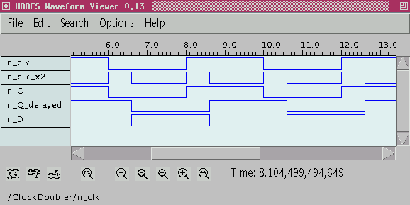
 Note that the duration of the 1-phase of the output clock signal
is the same as the delay through the delay inverters.
In a real circuit, the gate delay through the delay path will be
only a few nanoseconds, and therefore the duration of the
output clock pulses will also be only a few nanoseconds.