
Applets
contents
visual index
 introduction
 std_logic_1164
 gatelevel circuits
 delay models
 flipflops
 adders and arithm...
 counters
 LFSR and selftest
 memories
 ROM circuit
 1Kx8 ROM demo
 RAM structure
 RAM write-cycle
 RAM read-cycle
 RAM write-ha...
 RAM storage ...
 RAM address ...
 RAM bitline ...
 74189 SRAM
 74219 SRAM
 74219 SRAM a...
 6116 CMOS SRAM
 multiple SRAMs
 programmable logic
 state-machine editor
 misc. demos
 I/O and displays
 DCF-77 clock
 relays (switch-le...
 CMOS circuits (sw...
 RTLIB logic
 RTLIB registers
 Prima processor
 D*CORE
 MicroJava
 Pic16 cosimulation
 Mips R3000 cosimu...
 Intel MCS4 (i4004)
 image processing ...
 [Sch04] Codeumsetzer
 [Sch04] Addierer
 [Sch04] Flipflops
 [Sch04] Schaltwerke
 [Sch04] RALU, Min...
 [Fer05] State-Mac...
 [Fer05] PIC16F84/...
 [Fer05] Miscellan...
 [Fer05] Femtojava
 FreeTTS
The animation shown here runs for about 30 seconds; just re-start the simulator (click stop, then play) to watch the sequence again.
The timing of the write operations shown in the previous write-cycle demonstration first ensured that all address and data input values were stable, and the activated the nWriteEnable input to write the input data to the selected memory address. The nWriteEnable signal was then de-asserted before changing the data and address inputs again. This is the standard (and recommended) write operation.
However, it is also possible to modify the address and data inputs while the nWriteEnable is active (low). As the memory is built from latches (level-triggered), the memory cells are constantly overwritten with the current data input while the nWriteEnable signal is active. This is demonstrated during the first part of the animation sequence shown in this applet. First, the data inputs and address inputs are initialized to all zero; then the nChipSelect input is asserted (low) to select the memory chip. When the nWriteEnable input is activated (low), the RAM writes the current input data immediately to the selected memory cell (at address 0). Next, the address inputs are changed to addresses 01b, 10b, 11b, while nWriteEnable is kept low. This writes the data input value (0000b) to the selected memory cells in turn. Obviously, clearing the RAM with this operation is much faster when compared with the previous sequence, which would deactivate the nWriteEnable signal between the write operations.
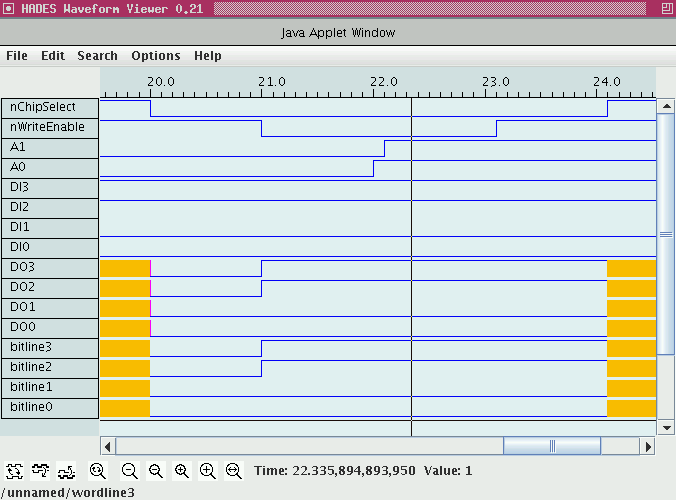
Unfortunately, the fast write operations cannot be used in general, due to hazard problems. This is demonstrated by the second part of the animation sequence. After the RAM has been cleared (see above), the data inputs are now set to the value (1100b). We want to write this data value to both the memory cells at address 0 (00b) and address 3 (11b). The demo sequence starts with address 00b and activates the nWriteEnable input, to correctly write the memory at address 0. While nWriteEnable is kept low, the address is now changed to 11b, which correctly writes the memory at address 3. However, it is impossible to guarantee that all address bits change at the same time. In the demo sequence, address bit A0 changes slightly before bit A1, and the resulting hazard implies that the data input value (1100b) is also written to memory address 1 (01b).
The following image shows the waveforms of the RAM during the write operation; note the slight timing difference of the address inputs which results in the unwanted writing to address 1 (left of the crosshair cursor):

Similar problems can occur if the nChipSelect and nWriteEnable inputs of RAM chips are driven by control signals that are not hazard-free. Even short 0-pulses on the nWriteEnable signal might be interpreted as valid write-commands by fast SRAM chips, randomly overwriting memory contents with whatever address- and data-inputs happen to be on its input pins at the time. Such problems can be very hard to debug. If in doubt, use additional flipflops to drive the nWriteEnable signals of RAM chips and use conservative write-cycle operations.