

Applets
contents
visual index
 introduction std_logic_1164 gatelevel circuits
 delay models
 gate vs. wir... gate delay d... ring oscillator hazards NAND-chain D-flipflop h... clock-doubler 2-phase cloc... flipflops adders and arithm... counters LFSR and selftest memories programmable logic state-machine editor misc. demos I/O and displays DCF-77 clock relays (switch-le... CMOS circuits (sw... RTLIB logic RTLIB registers Prima processor D*CORE MicroJava Pic16 cosimulation Mips R3000 cosimu... Intel MCS4 (i4004) image processing ... [Sch04] Codeumsetzer [Sch04] Addierer [Sch04] Flipflops [Sch04] Schaltwerke [Sch04] RALU, Min... [Fer05] State-Mac... [Fer05] PIC16F84/... [Fer05] Miscellan... [Fer05] Femtojava FreeTTS
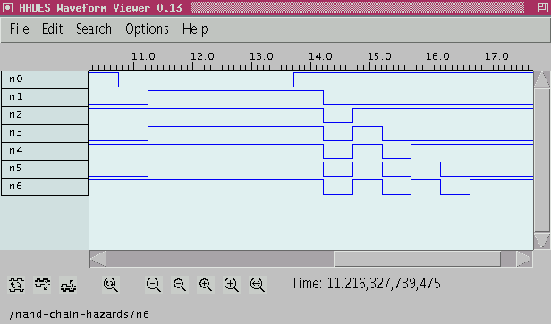 Note that circuit structures like this should be avoided
even if the rest of the system is designed to tolerate the hazards,
because the high amount of switching also implies a lot of
power consumption - at least for CMOS technology.
In fact, the most advanced logic synthesis systems include the option
to prefer low power consumption over low number of gates.
Challenge: Design a circuit that creates the maximum number of
hazards per number of gates :-)
Note that circuit structures like this should be avoided
even if the rest of the system is designed to tolerate the hazards,
because the high amount of switching also implies a lot of
power consumption - at least for CMOS technology.
In fact, the most advanced logic synthesis systems include the option
to prefer low power consumption over low number of gates.
Challenge: Design a circuit that creates the maximum number of
hazards per number of gates :-)