TAMS / Java / Hades / applets (print version): contents | previous | nextNAND-chain hazards demo
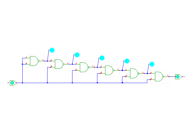 DescriptionThis circuit demonstrates that even a very simple circuit
with a only a few gates can create a lot of hazards.
Again, the gate delay of the individual gates is set to
a very large value (0.5 seconds), in order to provide
immediate visual feedback about the circuit operation.
Just toggle the input value and watch the behaviour.
When the input line is switched to a zero value, all NAND gates
generate a 1 output value (after one gate delay).
As soon as the input line is switched to a high value,
all gates see the logical 1 on their upper input from their
predecessor, and the logical 1 from the input line.
Therefore, all gates generate a logical 0 after one gate delay.
Only the first NAND gate is now stable, while the remaining
gates now have one input at zero, which implies that those gates
switch back to one.
This process repeats until the circuit finally stabilizes.
DescriptionThis circuit demonstrates that even a very simple circuit
with a only a few gates can create a lot of hazards.
Again, the gate delay of the individual gates is set to
a very large value (0.5 seconds), in order to provide
immediate visual feedback about the circuit operation.
Just toggle the input value and watch the behaviour.
When the input line is switched to a zero value, all NAND gates
generate a 1 output value (after one gate delay).
As soon as the input line is switched to a high value,
all gates see the logical 1 on their upper input from their
predecessor, and the logical 1 from the input line.
Therefore, all gates generate a logical 0 after one gate delay.
Only the first NAND gate is now stable, while the remaining
gates now have one input at zero, which implies that those gates
switch back to one.
This process repeats until the circuit finally stabilizes.
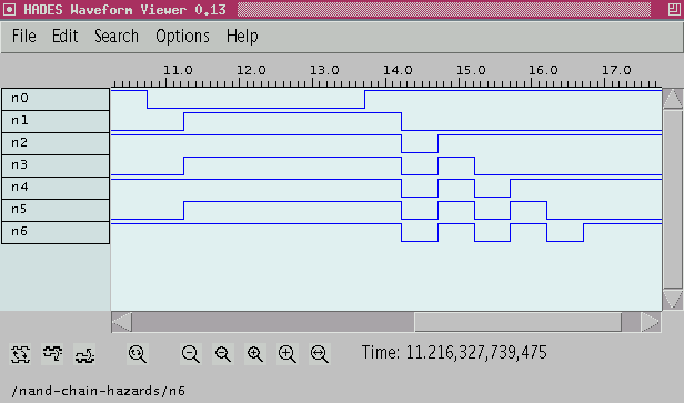 Note that circuit structures like this should be avoided
even if the rest of the system is designed to tolerate the hazards,
because the high amount of switching also implies a lot of
power consumption - at least for CMOS technology.
In fact, the most advanced logic synthesis systems include the option
to prefer low power consumption over low number of gates.
Challenge: Design a circuit that creates the maximum number of
hazards per number of gates :-)
Run the applet | Run the editor (via Webstart)
Note that circuit structures like this should be avoided
even if the rest of the system is designed to tolerate the hazards,
because the high amount of switching also implies a lot of
power consumption - at least for CMOS technology.
In fact, the most advanced logic synthesis systems include the option
to prefer low power consumption over low number of gates.
Challenge: Design a circuit that creates the maximum number of
hazards per number of gates :-)
Run the applet | Run the editor (via Webstart)
Impressum | 24.11.06
http://tams.informatik.uni-hamburg.de/applets/hades/webdemos/12-gatedelay/30-hazards/nandchain_print.html