
 |  |
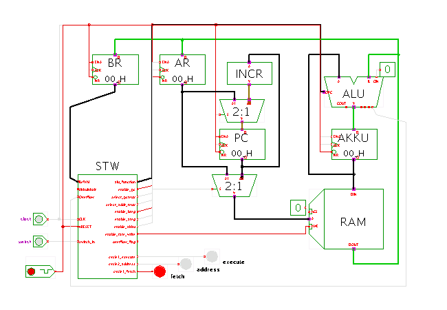
 DescriptionThis applets shows a RT-level circuit realization of the
PRIMA processor (primitive machine).
This simple 8-bit accumulator machine is used as a first example
of a von Neumann machine in our introductory lectures on computer science.
The 8-bit accumulator machine has the following main components:
The lower multiplexer decides whether the RAM address is taken from the program counter (during the fetch_instruction and fetch_address cycles), or from the address register (for load and store instructions).
The BR register holds the current instruction; its output value is the main input to the control unit (on the lower left) that generates the several register-enable and multiplexer-control signals. In order to avoid cluttering the schematics with dozens of control signals, all control signals are drawn as a single bus that runs on the top of the schematics and connects to the several registers and muxes.
A few links to further documentation:
NOTE: To keep the schematics as readable as possible, the version of PRIMA demonstrated in this applet is slightly different from the original version shown in the lecture slides. First, the applet uses an 8-bit ALU and accumulator register instead of the full 9-bit variants required by the original specification. Also, the carry-out from the ALU and the ALU output are not used in the control-unit. This saves a lot of bit-twiddling and a few global buses that would run across the whole schematics.
The demo program used in this applet consists of just four instructions:
label  addr  data  mnemonic
             (hex)
       0     0f    LD1
       1     00
loop:  2     0a    INCR
       3     00
       4     48    ST 20
       5     20
       6     80    BR 2
       7     02
The program first loads the value 1 into the accumulator.
It then increments the accumulator, store the result into
memory address 20, and jumps back to the increment instruction.
This is an endless loop, so that the program will continue to
increment the accumulator value and save it to the memory
over and over again.
Run the applet | Run the editor (via Webstart)