TAMS / Java / Hades / applets (print version): contents | previous | nextTTL-series 74151 multiplexer (8:1)
 DescriptionThis applet shows the circuit structure used
in the TTL-series 74151 8:1 multiplexer integrated circuit.
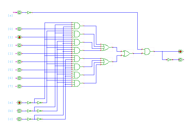
The circuit consists of eight AND gates whose outputs are then ORed
together by two stages of OR4 and OR2 gates.
The first three AND gate inputs are connected to the selection inputs
A,B,C or the inverted values of A,B,C.
The final input of each AND gate is connected to the corresponding
data input D0..D7.
For example, if the selection inputs are C=0, B=0, A=1,
only the AND gate connected to D1 will have at logical 1 at each of
its upper three inputs. Therefore, all other AND gates generate a 0 output.
The D1 AND gate, however, will propagate the D1 input value to the
OR gates and therefore to the multiplexer output.
The same argument holds for each of the remaining seven selection
input combinations.
The addional strobe input allows to deactivate the whole multiplexer.
Due to the final AND gate, the Y output will always be 0 unless
the strobe input is 0.
The W output simply provides the inverted Y ouptut value.
Run the applet | Run the editor (via Webstart)
Impressum | 24.11.06
http://tams.informatik.uni-hamburg.de/applets/hades/webdemos/10-gates/40-mux-demux/SN74151_print.html


 DescriptionThis applet shows the circuit structure used
in the TTL-series 74151 8:1 multiplexer integrated circuit.
The circuit consists of eight AND gates whose outputs are then ORed
together by two stages of OR4 and OR2 gates.
The first three AND gate inputs are connected to the selection inputs
A,B,C or the inverted values of A,B,C.
The final input of each AND gate is connected to the corresponding
data input D0..D7.
For example, if the selection inputs are C=0, B=0, A=1,
only the AND gate connected to D1 will have at logical 1 at each of
its upper three inputs. Therefore, all other AND gates generate a 0 output.
The D1 AND gate, however, will propagate the D1 input value to the
OR gates and therefore to the multiplexer output.
The same argument holds for each of the remaining seven selection
input combinations.
The addional strobe input allows to deactivate the whole multiplexer.
Due to the final AND gate, the Y output will always be 0 unless
the strobe input is 0.
The W output simply provides the inverted Y ouptut value.
Run the applet | Run the editor (via Webstart)