
 |  |
 Description
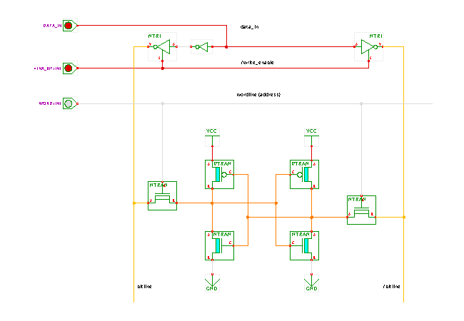
A switch-level demonstration of the typical six-transistor
SRAM storage cell.
Click the input switches of type the 'd' bindkey to control the DATAIN data input value, 'e' to enable the bitline tristate drivers, and 'w' to control the wordline.
The memory cell shown here forms the basis for most static random-access memories in CMOS technology. It uses six transistors to store and access one bit. The four transistors in the center form two cross-coupled inverters. In actual devices, these transistors are made as small as possible to save chip-area, and are very weak. Due to the feedback structure, a low input value on the first inverter will generate a high value on the second inverter, which amplifies (and stores) the low value on the second inverter. Similarly, a high input value on the first inverter will generate a low input value on the second inverter, which feeds back the low input value onto the first inverter. Therefore, the two inverters will store their current logical value, whatever value that is.
The two lines between the inverters are connected to two separate bitlines via two n-channel pass-transistors (left and right of the cell). The gates of those transistors are driven by a wordline. In a larger SRAM, the wordline is used to address and enable all bits of one memory word (e.g. all 32 bits at address 0xcafe from a 64Kx32 SRAM chip). As long as the wordline is kept low, the SRAM cell is disconnected from the bitlines. The inverters keep feeding themselves, and the SRAM stores its current value.
When the wordline is high, both n-channel transistors are conducting and connect the inverter inputs and outputs to the two vertical bitlines. That is, the two inverters drive the current data value stored inside the memory cell onto the bitline (left) and the inverted data value on the inverted-bitline (right). This data can then be amplified and generates the output value of the SRAM cell during a read operation.
To write new data into the memory, the wordline is activated, and the strong bitline input-drivers (on top of the schematics) are activated. Depending on the current value stored inside the SRAM cell there might be a short-circuit condition, and the value inside the SRAM cell is literally overwritten. This only works because the transistors inside the SRAM cell are very weak.
Note: a single bitline and a transmission-gate could also be used to access the memory data, but two n-channel transistors are smaller and faster than one transmission-gate.
   DIN  nWE  wordline  |  Bitline  data+ (new data)
  ---------------------+--------------------------------------
     *    1         0  |  Z        data  (cell passive, stores)
     *    1         1  |  data     data  (read cell)
     0    0         0  |  0        data  (cell passive, stores)
     1    0         0  |  1        data  (cell passive, stores)
     0    0         1  |  0        0     (write 0)
     1    0         1  |  1        1     (write 1)
Further reading: Please also check the corresponding gate-level SRAM demonstrations in the memories chapter of this applet collection. Click here for the overview page with the SRAM architecture. An interactive applet demonstration of the 6T-cell can be found here. Besides the use of only six transistors to store one-bit of information, the 6T-cell also allows for a very compact routing of signal wires.
Run the applet | Run the editor (via Webstart)