TAMS / Java / Hades / applets (print version): contents | previous | nextUSART 8251 transmitter demonstration
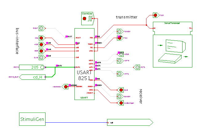
 DescriptionThis applet demonstrates the transmitter block of the
USART 8251 or
universal synchronous and asynchronous receiver and transmitter.
For an overview and register description of the USART chip,
please visit the 8251 overview applet page.
As you can see, the circuit shown in the applet uses a single 8251 chip,
with its TXD data output connected to
the RX receiver input of a serial terminal.
Therefore, characters transmitted by the 8251 will be decoded
and displayed by the terminal, as long as the communication settings
of the transmitter and the terminal match.
The TXC inputs of the 8251 is driven by a clock generator
which is set to a clock period of 1.6667 msec or 600 baud.
A stimuli generator component is used to automatically initialize
the USART for transmission and to demonstrate the timing
of the transmitter and its status signals.
The communication parameters of both the 8251 and the terminal
are set to eight databits, no parity, and two stopbits.
Once the simulation starts, the stimuli generator component
applies the following sequence of input changes to the circuit:
- all signals of the 8251 bus-interface are initialized
to their inactive values.
- a 0-1-0 pulse is generated on the RESET signal to initialize
the 8251 chip to a well-defined state.
- a value of 0xcd is written into the 8251 mode register,
which selects asynchronous communication mode with eight databits,
no parity, and two stopbits - or 8N2 for short.
Remember that the first command write operation following a reset
is interpreted as a write operation to the mode register.
Also, please check the typical system bus write sequence:
first, the nCS chip-select signal is asserted (active low),
then the 8-bit value 0xcd is applied to the data-bus,
CnD is asserted (high) to select a command transfer,
and finally a short 1-0-1 pulse is generated on the nWR write-enable
input.
- a value of 0x11 is written into the 8251 command register.
Again, CnD is kept high, nCS is asserted low, the value 0x05
is applied to the databus, and a 1-0-1 pulse on the nWR signal
executes the write operation.
The value 0x11 activates the transmitter and disables the
on-chip receiver. Also, the parity/frame/overrun error flags
in the status register are reset.
- it follows a read operation to check the 8251 status register.
To avoid a short-circuit condition on the data bus, the stimuli
generator first tristates the bus.
Again, nCS is asserted low to activate the chip and CnD is kept high
to select a status register read operation.
Note that the 8251 drives the data-bus while the nRD signal
is kept low.
The returned value of 0x84 shows that the nDSR input is kept low
(bit D7 set),
while the transmitter is empty (bit D2 set)
and both receiver and transmitter are ready (bit D1 and D0 cleared).
- A value of 0x55 is written to the transmit buffer register of the
8251 to initiate a first data transfer.
This time, the CnD signal is kept low to select a data transfer
while nCS is kept low to select the 8251 chip.
Again, a 1-0-1 pulse on the nWR signal completes the write cycle.
Because the nCTS signal is asserted (low), the transmitter begins
transmitting the startbit on the next falling edge of the nTXC
transmitter clock. The eight databits and the two stopbits are
generated and transmitted during the following ten cycles of the
nTXC signal.
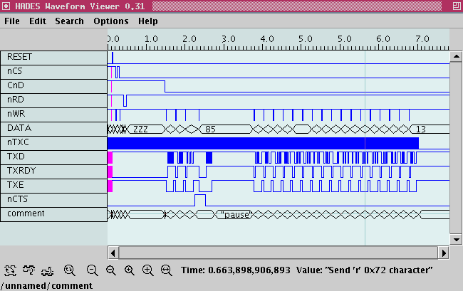
Please check the waveforms to verify that the TXE (transmitter
empty) output signal is asserted once the transmitter begins
the actual transmission with the startbit.
However, the TXRDY (transmitter ready) signal is asserted much later
after the second stopbit has been transmitted.
- A value of 0xAA is now written to the transmit buffer to
initiate another data transfer.
- A value of 0x33 is now written to the transmit buffer to
initiate another data transfer.
The bit sequence of those two write operations is chosen to make
the structure of the startbit-databits-stopbit sequence explicit.
- The nCTS signal is now de-asserted (high), and another
value of 0x55 is written to the data register.
Note that the transmission is blocked because nCTS (clear-to-send)
is de-asserted.
However, once nCTS goes low, the transmission starts on the next
falling edge of the nTXC clock input.
- A short phase of inactivity is introduced, to make the following
group of transmissions easy to identify in the waveforms.
- The string "\nHello, world\n" is transmitted via the USART:
0x0a 0x0d 0x48 0x65 0x6c 0x6c 0x6f 0x2c 0x20 ...
When the automatic sequence has finished,
you should take a look at the signal waveforms
to check and understand the RS-232 datastream
and the values returned by the status register read operations.
The waveform of the extra comment signal includes a
short description of the ongoing operation.
Just click the repaint button in the waveform viewer to update
the waveforms, and use the zoom buttons or the zoom-region option
to enlarge the areas of interest.
For easy comparison between data bus values and transmitter waveforms,
you might want to select hexadecimal number format in the waveform
viewer (via menu, options, number format, hex).
The screenshot below shows example waveforms during the first
block of transmitted characters.

You can also click on the symbol of the serial terminal component,
to open (or close) the user-interface window of the terminal
and check that the transmitted data characters were indeed received
correctly.
To further explore the circuit,
just continue the simulation via clicking the "run" button
(play) in the simulator control panel.
You can now use the DATA input switch and the nWR write-enable switch
to transmit other data characters via the USART chip.
You can also type the following bindkeys to control the applet:
'r' for nRD, 'w' for nWR, 'x' for RESET.
Run the applet | Run the editor (via Webstart)
Impressum | 24.11.06
http://tams.informatik.uni-hamburg.de/applets/hades/webdemos/50-rtlib/65-usart8251/usart-transmit_print.html


 DescriptionThis applet demonstrates the transmitter block of the
USART 8251 or
universal synchronous and asynchronous receiver and transmitter.
For an overview and register description of the USART chip,
please visit the 8251 overview applet page.
