TAMS / Java / Hades / applets (print version): contents | previous | nextTTL-series 74189 SRAM demonstration
 DescriptionThis applet demonstrates the
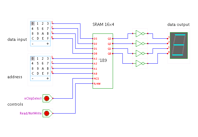
TTl-series 74189 16x4 bit SRAM circuit.
The memory matrix consists of 64 latches organized as 16 (2^4) words
of 4 bits each, accessible via separate input and output lines.
A 4 bit address input selects one of the 16 memory words.
Note: for some obscure implementation reason, the actual 7489 and 74189 RAM
integrated circuits use inverted outputs - the values on the
output bus are the inverse of the data previously written into the RAM.
Another chip in the TTL-series of integrated circuits, called the 74219,
was otherwise identical to the 7489 and 74189 circuits, but used
non-inverting data outputs.
See the 74219 demonstration applet
to compare the behaviour of the RAM chips.
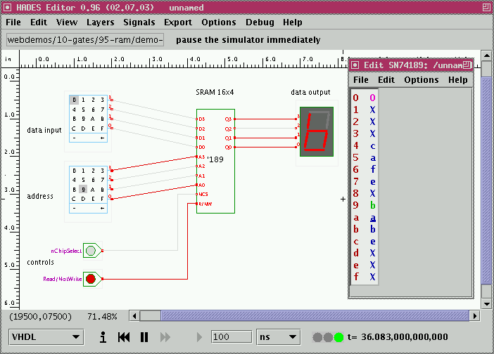
Use the property editor (popup menu->edit) to open the user interface
with the memory editor. It shows a table with the current memory data
contents (hex encoded), with the memory addresses on the left and
the data stored at the address on the right.
Additionally, the memory word last read and written are highlighted
in green and cyan colors (unless you use a personalized color scheme).
To edit the RAM contents, move the mouse to the memory cell in question,
click the left button, and then enter the new value as a hexadecimal
number via the keyboard. The 74189 RAM only stores 4-bit per memory word,
so that a single keystroke ('0' .. '9', 'a' .. 'f') is sufficient.
The following screenshot shows the Hades editor running the 74189
RAM demo with the memory editor open:
DescriptionThis applet demonstrates the
TTl-series 74189 16x4 bit SRAM circuit.
The memory matrix consists of 64 latches organized as 16 (2^4) words
of 4 bits each, accessible via separate input and output lines.
A 4 bit address input selects one of the 16 memory words.
Note: for some obscure implementation reason, the actual 7489 and 74189 RAM
integrated circuits use inverted outputs - the values on the
output bus are the inverse of the data previously written into the RAM.
Another chip in the TTL-series of integrated circuits, called the 74219,
was otherwise identical to the 7489 and 74189 circuits, but used
non-inverting data outputs.
See the 74219 demonstration applet
to compare the behaviour of the RAM chips.
Use the property editor (popup menu->edit) to open the user interface
with the memory editor. It shows a table with the current memory data
contents (hex encoded), with the memory addresses on the left and
the data stored at the address on the right.
Additionally, the memory word last read and written are highlighted
in green and cyan colors (unless you use a personalized color scheme).
To edit the RAM contents, move the mouse to the memory cell in question,
click the left button, and then enter the new value as a hexadecimal
number via the keyboard. The 74189 RAM only stores 4-bit per memory word,
so that a single keystroke ('0' .. '9', 'a' .. 'f') is sufficient.
The following screenshot shows the Hades editor running the 74189
RAM demo with the memory editor open:
 The behaviour of the 74189 circuit is controlled by just two active-low
control lines, namely the chip select and read/write
inputs:
The behaviour of the 74189 circuit is controlled by just two active-low
control lines, namely the chip select and read/write
inputs:
- nCS=1: the data outputs are tri-stated and the clock signal
for the latches in the memory matrix is disabled.
- nCS=0, Read/nWrite=1:
the data outputs are enabled and driven with the contents
of the currently addressed memory word.
When the address input is changed, the contents of the
newly selected memory word will appear on the data outputs,
delayed by the memory access time.
- nCS=0, Read/nWrite=0:
the clock signal of the currently addressed memory latches
is enabled, so that the values on the data input bus
is copied into the selected memory word (transparent latches).
Also, the data outputs are enabled.
Switch the Read/nWrite signal back to the high (1) state
to store the data.
To get accustomed to the behaviour of the SRAM, it is a good exercise
to try to write a few data words into the memory (e.g. the values
shown in the screenshot above).
Due to the asynchronous interface of the RAM, great care must be
taken to avoid hazard conditions on either of the Read/nWrite and
address inputs.
A good example is provided by the following procedure to clear all RAM
contents:
1. clear the data inputs (value 0000),
2. enable the Read/nWrite signal (value 0),
3. step through all addresses.
Needless to say that such tricks are not recommended for real system
designs...
Run the applet | Run the editor (via Webstart)
Impressum | 24.11.06
http://tams.informatik.uni-hamburg.de/applets/hades/webdemos/40-memories/40-ram/demo-74189_print.html