

| |
 Description
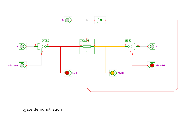
A demonstration of the CMOS transmission-gate.
Description
A demonstration of the CMOS transmission-gate.
Click the input switches or type the ('a','x'), ('b','y'), and ('s') bindkeys to control the circuit.
The CMOS transmission-gate (or tgate for short) works like a voltage-controlled switch, similar to an electromagnetical relay with one normally-open contact. It consists of one n-channel and one p-channel transistors with common source and drain connections. In the Hades simulation models, these are the left and right ports, called A and B. In actual transmission-gates, the gates of the two transistors are controlled by separate input signals, C and NC, which are expected to be inverse to each other. The idea is that a high voltage (logical 1) on its gate activates the n-channel transistors, while the p-channel transistor conducts when a low voltage (logical 0) is applied to its gate. On the other hand, both transistors are non-conducting when a low voltage (logical 0) is applied to the gate of the n-channel transistor while a high voltage (logical 1) is applied to the gate of the p-channel transistor. This can be summarized by the following function table:
   C   NC   |  switch
 -----------+-----------
   0   1    |  open    (no connection between A and B)
   1   0    |  closed  (A and B connected)
            |
   0   0    |  weak conducting (low voltage, not used in practice)
   1   1    |  weak conducting (high voltage, not used in practice)
The latter two states (C=NC=0 and C=NC=1) are not used in practice, because only one transistor would be conducting with the complementary transistor non-conducting. (It would be cheaper to use just a single pass-transistor instead of the two-transistor t-gate). Also, the current switch-level simulation algorithm in Hades cannot accurately model those states. Therefore, only the positive C input is used by the Hades transmission-gate component simulation model. The inverted NC input is still indicated on the symbol, but not used. (This also allows simplifying the schematics, because the NC signal can be drawn, but must not.)
In the circuit shown here, the tgate gate input is controlled by input switch S, while the A and B ports of the tgate are connected to a tri-state buffer each. This allows you to apply either of a logical 0, logical 1, or logical Z to each side of the tgate and observe the corresponding behavior.
Run the applet | Run the editor (via Webstart)