
 |  |
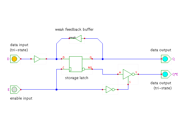
 DescriptionThis applet demonstrates the behaviour of a 1-bit storage cell
inside a typical
random access memory (RAM).
The RAM applet
uses 16 of these cells as its memory.
The storage element shown in the applet is a standard D-type latch. The data input to the latch is connected to both the bit-line input and the weak feedback buffer. As long as the E-line is disabled, the flipflop clock input is low and the flipflop keeps its current value.
When the E-line input is enabled, the flipflop becomes transparent, while the actual voltage on the data input line of the flipflop depends on the (Kirchhoff-laws!) output of the (weak) feedback buffer and the (strong) external data input.
While it is possible to construct a memory cell as shown in the applet, the six-transistor SRAM and one-transistor DRAM cells are much more compact. Therefore, the latch-based memory cell is only used rarely in practice.
An interactive applet demonstration of the 6T-cell can be found here. Besides the use of only six transistors to store one-bit of information, the 6T-cell also allows for a very compact routing of signal wires.
(Note: if you look closely, you will observe that the buffer inserted between bitline data input and latch data input behaves different from a standard non-inverting buffer in Hades: it transforms a 'Z' input value into a 'Z' output value, while the standard buffer would generate a 'X'. In the actual RAM cell, both this special input buffer and the tri-state output buffer are realized with MOS pass-transistors connected to the bitline(s). Using this 'fake' buffer avoids to introduce a pass-transistor model for the demo.)
Run the applet | Run the editor (via Webstart)