
 |  |
 Description
This applet demonstrates the typical SRAM read- and write-access
operations with a predefined animation
driven by a stimuli generator component.
The simulation is slowed-down to allow you to watch and observe
all memory accesses.
You may want to open the memory editor (popup menu, edit component)
to watch the memory contents during the animation sequence.
Use the simulator control buttons (pause, rewind, start) to
pause and restart the animation.
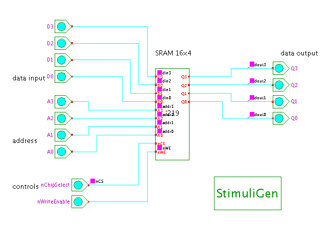
The circuit shown here consists of a single SRAM chip, a few input switches and output LEDs, and the StimuliGenerator component. The latter generates the input data for the SRAM during the simulation. Because of its small size and fully static operation, the TTL-series 74219 16x4 bit SRAM circuit is used for the demo. Please visit the 74219 demonstration applet page for a fully interactive demonstration of the 74219 chip without predefined animation.
Initialization: The simulation starts with all inputs in the undefined state. We then initialize the SRAM control inputs (chip-select and write-enable) to the 1 state to disable the SRAM. Next, the data inputs are initialized to the 0101 (value 5) states, and the address inputs are initialized to address 0000.
Chip select: The animation then enables the SRAM via nChipSelect=0. Because the SRAM chip contains to valid data at this time, the data outputs are still undefined.
First write cycle: and starts a write-cycle via setting nWriteEnable=0 and then nWriteEnable=1 while the address inputs read 0000 and the data inputs 0101. This writes the value 5 into the memory cell at address 0. Note that the data outputs now also immediately reflect the new data value of the addressed memory cell.
Second write cycle: Next, the address bus changes to the value 0001, while the data bus is held at the value 0101. A second write cycle is executed via nWriteEnable=0 and nWriteEnable=1. The memory at address 1 now also holds the data value 5 (0101).
Third write cycle: We now change the data input to the value 1001 (9), and the address input to 1111 (F). Another cycle of nWriteEnable=0 and nWriteEnable=1 writes the data value 9 into address 1111.
Write remaining RAM cells: The following write cycles write the data value 0000 into memory cells 0010, 0011, and 0100. We now change Read cycles: Finally, the animation read the memory data from address 1111 and the adress 0000.
Run the applet | Run the editor (via Webstart)