
 |  |
 Description
This applet demonstrates the internal structure of a
read-only memory or ROM.
A rather small memory size of 16 words of 8 bits each is used.
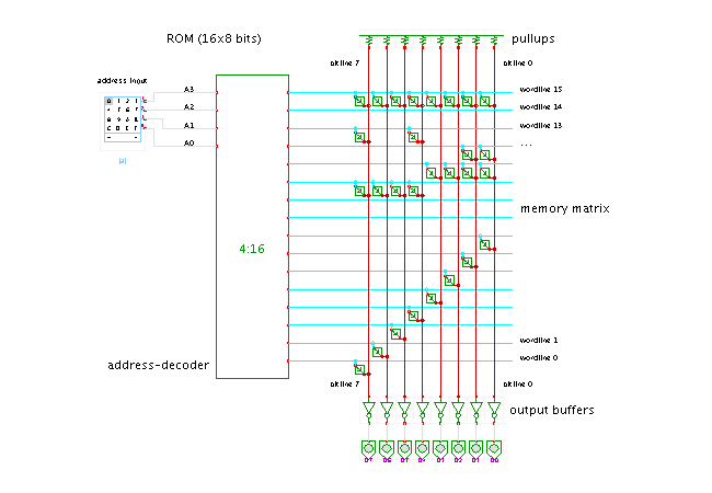
From left to right, the circuit consists of three stages.
The first stage, usually called address-decoder in memory circuits,
is a standard demultiplexer.
For each binary address input pattern, exactly one of the
wordlines (horizontal) is activated by the address-decoder.
In the example, a 4-to-16 demultiplexer is required
to control the 16 wordlines corresponding to the 16 memory addresses.
The memory matrix is the main part of the ROM.
For each wordline, a connection is made to those bitlines (vertical)
that should be activated for the corresponding memory word.
In bipolar technology, simple diodes can be used to make the
connections of wordlines to bitlines.
However, usually transistors are used to amplify the wordline signal.
In MOS technologies, N-type transistors are preferred, because they are faster than P-type transistors of the same size. The transistor gate is connected to the wordline, drain to the bitline, and the transistor source to Vss (ground). This results in the wired-AND structure shown in the applet. The pullup resistors on each bitline drive the bitline to a weak high voltage (logical H), when no transistors are active. If a transistor is used at the connection of a wordline and bitline, the transistor will conduct whenever the wordline is active, driving the bitline to a low voltage (logical 0).
As N-type transistors are used in the memory matrix, an active bitline is driven to zero voltage, while an inactive bitline remains at (weak) high. Therefore, an additional stage of amplifiers and output buffers is required to generate a strong output signal. The applet uses a single stage of inverters. All together, the ROM shown in the applet implements the following logical function:addr A3 A3 A1 A0 D7 D6 D5 D4 D3 D2 D1 D0 15 1 1 1 1 1 1 1 1 1 1 1 1 14 1 1 1 0 0 0 0 0 0 0 0 0 13 1 1 0 1 1 0 0 1 0 0 0 0 12 1 1 0 0 0 0 0 0 0 0 1 1 11 1 0 1 1 0 0 0 0 1 1 1 1 10 1 0 1 0 1 1 1 1 0 0 0 0 9 1 0 0 1 0 0 0 0 0 0 0 0 8 1 0 0 0 0 0 0 0 0 0 0 0 7 0 1 1 1 0 0 0 0 0 0 0 1 6 0 1 1 0 0 0 0 0 0 0 1 0 5 0 1 0 1 0 0 0 0 0 1 0 0 4 0 1 0 0 0 0 0 0 1 0 0 0 3 0 0 1 1 0 0 0 1 0 0 0 0 2 0 0 1 0 0 0 1 0 0 0 0 0 1 0 0 0 1 0 1 0 0 0 0 0 0 0 0 0 0 0 1 0 0 0 0 0 0 0Due to electrical reasons it is difficult to connect more that a few hundred transistors to one bitline or wordline. Therefore, larger ROMs use a slightly different architecture, with a set of smaller memory blocks instead of one single large memory block. Each memory block uses approximately the same number of wordlines and bitlines (the applet has 16 wordlines and 8 bitlines). For example, a good size for one memory block might consist of 256 wordlines and 256 bitlines. This means that a 64Kx8 bit ROM would be organized internally as a set of (65536x8) / (256x256) = 8 memory blocks. The top 3 address bits select the memory block to use, the next 8 bits select the wordline to use, and the remaining 5 address bits select which part of the memory block output of 256 bits is to be sent to the 8 data outputs. Run the applet | Run the editor (via Webstart)