

| |
 DescriptionThis applet demonstrates a hardware-realization of a
stack memory.
A standard asynchronous RAM component is used as the actual memory,
while the remaining components implement the stack controller.
DescriptionThis applet demonstrates a hardware-realization of a
stack memory.
A standard asynchronous RAM component is used as the actual memory,
while the remaining components implement the stack controller.
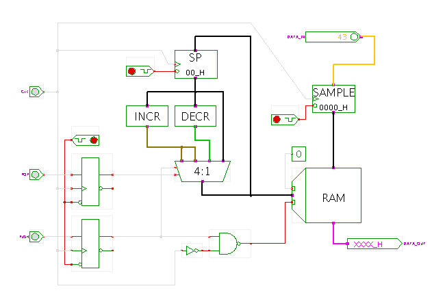
The circuit shown here is usually called a single-cycle clocked stack (scstack) in datasheets, due to its clocked operation. All of the input ports of the stack are sampled on the rising edge of the input clock signal. These are the n-bit data input and the two (active high) command inputs push and pop.
Click the input switches or type the 'c' (clock), 'p' (push), and 'o' (pop) bindkeys to play with the stack. Also click the DATA_IN switch to change the data written into the stack between push operations. Open the memory editor (popup-menu, edit component) to watch the data written to and read from the RAM component. (The next applet includes a variant of the scstack circuit where the clock signal and the data input are driven by a clock generator and a counter.)
If neither push nor pop are high during the rising edge of the clock signal, the 4:1 multiplexer control bits are (00) and the current contents of the stack-pointer register SP are passed through to the multiplexer output. Therefore, the data memory RAM will output the contents of the memory cell addressed by SP; this is the current top-most entry of the stack. The SP register will be re-loaded with its current value on the next rising edge of the clock signal; this is equivalent to a no-operation.
If the pop signal is high during the rising edge of the clock, the 4:1 multiplexer passes the output value of the decrementer block. The RAM now outputs the contents of the memory cell addressed by (SP-1), and the SP register will be decremented on the next rising edge of the clock input. This performs the pop operation of the stack. Note that the circuit shown here includes no logic to detect or avoid popping data from an empty stack. If the stack pointer overflows, invalid data will be read from the stack.
If the push signal is high during the rising edge of the clock, the 4:1 multiplexer passes the output of the incrementer block. This means that the RAM is now addressed by (SP+1), and the SP register will be incremented on the next rising edge of the clock input. It now remains to actually write the input data from the SAMPLE register into the RAM memory. This is done with the extra logic at the bottom of the schematics. The NAND-gate ensures that the write-enable input of the RAM is active (low) while the push-flipflop is high and the clock signal is low. Therefore, the stack will output an invalid value during a push-operation while the clock input is high (the RAM is addressed by SP+1, which contains no valid data yet). Only when the clock signals goes low is the new data written to the RAM, and the stack output becomes valid.
Note that the circuit includes no logic to detect or avoid pushing data into a full stack; instead, previously written data will be overwritten with the current input data. Also, the first data value is written to address one instead of address zero, because the stack pointer is first incremented.
As usual, the timing of the RAM write-enable signal is criticial. As shown here, the combined delay of the 4:1 multiplexer and incrementer must be lower than the high-time of the clock signal, and the delay of the write-enable logic (NAND-gate and inverter) must be lower than the delay of the multiplexer and the propagation delay of the SAMPLE buffer register. Another clocking strategy would be to derive the write-enable signal directly from the push-flipflop output, instead of using the low-time of the clock signal. However, this requires a delay-line to ensure that write-enable only becomes active after the incremented address is available. In practice, the operating frequency of the stack might be limited by the carry-propagation delay of the incrementer and decrementer blocks, so that carry-lookahead adders might be required for fast operation.
Due to the 4:1 multiplexer-connections and the write-enable logic based on the push-flipflop, the stack will perform a standard push operation when both push and pop inputs are high during the rising edge of the input clock.
The circuit shown here has been kept as simple as possible. A 'real' stack controller would include additional logic to fix the following flaws:
Run the applet | Run the editor (via Webstart)