
 |  |
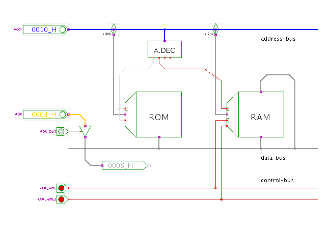
 DescriptionA demonstration of a simple (but typical) microprocessor system bus,
built with RTLIB simulation components.
In most microprocessor systems, all main components are connected
via buses to save signal wires and circuit-board space.
Usually, separate buses are provided to transmit memory addresses
(the address-bus), data (data-bus),
and control signals (control-bus).
In the applet, both the address bus (on top) and data bus (bottom) are 16 bit wide and run from the left to the right. Instead of a microprocessor, input switches (on the left) are provided to control the buses. In a typical system, dozens of different memory and I/O-components as well as the microprocessor would be connected to the bus, but the applet only uses one ROM and one RAM component in addition to the input switches. In a memory-mapped system, the individual components are enabled based on the current memory-address provided by the microprocessor (or the addr switch in this applet).
The address-decoder component is set to enable the ROM component
for the memory address range 0x0000 .. 0x07ff
(corresponding to 1024 memory words),
and to enable the RAM component for the memory address range
0x0800 .. 0x0fff (another 1024 memory words).
Please check the previous applet for a discussion and demonstration
of the byte-vs-word-address strategy.
The bus-tap components between the address bus and the ROM and RAM
components select the required subset of address bits to address
the memory (here, 1024 words per memory component).
For addresses between 0x1000 .. 0xffff,
the address-decoder enables neither RAM nor ROM.
This range could be used to add more components to the system.
Instead of a full-blown control bus, only two additional signals are provided in the applet. The RAM_nWE and RAM_nOE signals are connected to the corresponding RAM inputs and allow you to select either read or write operations while the address-decoder enables the RAM (address range 0x0800 .. 0x0fff).
(Note: Some bus-systems like the 32-bit PCI bus architecture don't use separate address- and data-signals, but transmit both addresses and data of the same time-multiplexed wires. To reduce the performance penalty of having to transmit all addresses and data over the same signals wires, burst-modes are usually provided on such buses, where multiple data transfers are performed after transferring only the first address. Recently, high-speed serial-bus systems like USB and Firewire have become wide-spread. These use elaborate packed-based protocols to transmit all commands and data over only a single or a few signal lines.)
Run the applet | Run the editor (via Webstart)