

| |
 DescriptionOne of the most important aspects of electronics circuits modelling
concerns if and how to describe circuit timing.
On the lower abstraction levels, the circuit behavior can be modelled
very accurately via systems of differential equations for the
voltages and currents in the devices.
Those equations can include temperature and other environmental effects,
and even circuit aging or electromigration.
Unfortunately, solving the differential equations is
computationally very expensive and is impractical on large circuits.
Also, the level of detail created by such simulations is extremely high.
For example, a digital designer usually is not interested in the actual
voltages at the gate outputs, as long as the voltage is within the bounds
for the logical low or high values at the required time.
Therefore, other modelling techniques have to be used on the higher
abstraction levels.
The simplest scheme for clocked circuits is simply to count clock
cycles and to ignore all timing details within a clock cycle.
This implies that timing information, e.g. to determine the maximum
clock rate, will have to be created with other tools.
However, such cycle-based (in German: periodenorientiert)
simulations can be made to run very fast on standard workstations
and use (comparatively) little memory.
Therefore, cycle-based simulation has recently become the preferred
method to simulate large circuits like modern microprocessor systems.
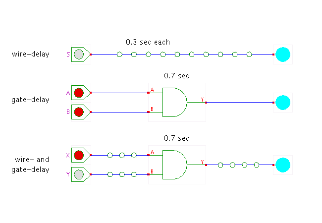
Naturally, each logical gate needs some time before its output
stabilizes after input changes.
This motivates the gate-delay model, where each component
in a circuit is assigned a set of delay values.
Those delays can be taken from actual device measurements or
from device simulations.
For example, a two-input NAND gate in a 1.0 micron CMOS process
might be assigend a single delay value of 5 nanoseconds.
However, the new gate output value also needs some time to travel
across the output wire before it reaches the next gates.
This wire propagation delay can be computed accurately
once the actual wire layout of a chip (or circuit board) is known
- which is not true during the early design stages.
Therefore, the wire delays are often approximated by the number
of components connected to the wire and a coarse estimate
for wire length between components.
The example applet demonstrates those delay models:
DescriptionOne of the most important aspects of electronics circuits modelling
concerns if and how to describe circuit timing.
On the lower abstraction levels, the circuit behavior can be modelled
very accurately via systems of differential equations for the
voltages and currents in the devices.
Those equations can include temperature and other environmental effects,
and even circuit aging or electromigration.
Unfortunately, solving the differential equations is
computationally very expensive and is impractical on large circuits.
Also, the level of detail created by such simulations is extremely high.
For example, a digital designer usually is not interested in the actual
voltages at the gate outputs, as long as the voltage is within the bounds
for the logical low or high values at the required time.
Therefore, other modelling techniques have to be used on the higher
abstraction levels.
The simplest scheme for clocked circuits is simply to count clock
cycles and to ignore all timing details within a clock cycle.
This implies that timing information, e.g. to determine the maximum
clock rate, will have to be created with other tools.
However, such cycle-based (in German: periodenorientiert)
simulations can be made to run very fast on standard workstations
and use (comparatively) little memory.
Therefore, cycle-based simulation has recently become the preferred
method to simulate large circuits like modern microprocessor systems.
Naturally, each logical gate needs some time before its output
stabilizes after input changes.
This motivates the gate-delay model, where each component
in a circuit is assigned a set of delay values.
Those delays can be taken from actual device measurements or
from device simulations.
For example, a two-input NAND gate in a 1.0 micron CMOS process
might be assigend a single delay value of 5 nanoseconds.
However, the new gate output value also needs some time to travel
across the output wire before it reaches the next gates.
This wire propagation delay can be computed accurately
once the actual wire layout of a chip (or circuit board) is known
- which is not true during the early design stages.
Therefore, the wire delays are often approximated by the number
of components connected to the wire and a coarse estimate
for wire length between components.
The example applet demonstrates those delay models:
(Note: due to its simulation algorithm, Hades cannot really model wire-delays. The small delay-nodes are actually just standard simulation components, each of which uses the gate-delay model. Still, you should get the idea of electrical waves traveling along the signal wire as the source of delay).