
 |  |
 Description
This applet demonstrates a very compact but tricky realization
of an XOR gate based on a CMOS transmission gate.
Click the input-switches or type the 'a' and 'b' bindkeys to control the circuit.
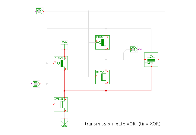
The circuit shown here realizes the XOR function of inputs A and B using just six transistors. The first stage of the circuit consists of a basic static inverter, which generates the inverse of input A. Note that the inverse of A is connected to the gate of the transmission-gate n-channel transistor, while A is connected to the gate of the p-channel transistor. Therefore, the transmission gate is conducting when A is low, and passes the value of B. This effectively realizes the (!A & B) term of the standard disjunctive expansion of the XOR function.
In order to realize the remaining (A & !B) term of the XOR expansion, the circuit uses a dirty trick. Obviously, the two transistors in the center of the schematics form an inverter that calculates !B, and whose output is connected to the output of the XOR gate. However, the source and drain connections of the transistors are not directly connected to VCC and GND, but to the input A and the output !A of the first-stage inverter. The net result is that the inverter is only active when A is high, because its power-supply is effictively switched-off when A is low.
Similiar realizations are possible for a variety of logical functions. (For example, reversing the gate connections of the transmission-gate and switching the transistors of the middle inverter gives the XNOR function). However, while such circuits usually are much more compact than the logically equivalent static gates, they are also less robust and should be used with great care. For example, using the output of other gates as the power-supply obviously decreases the voltage levels and maximum currents, with corresponding loss of noise immunity and maximum load of the gate. Also, extra buffers might be necessary between stages of gates built with transmission-gates, to compensate for the non-ideal transmission characteristics.
Note: circuits like this are notoriously hard to simulate. It is actually rather a coincidence that the circuit shown here can be simulated within the simple switch-level model. When A is low, the middle inverter is turned off in the real circuit, due to the weak-conducting behavior of the actual MOS transistors, while the Hades simulation model does not care about this situation. This does no harm here, because the transistors modeled as conducting propagate the same value as the value propagated by the t-gate. Before relying on circuits like this, the behavior must be checked with detailed device-level simulators like SPICE.
Run the applet | Run the editor (via Webstart)