
 |  |
 Description
This applet shows another way to draw the CMOS transmission-gate latch
presented and explained in the previous applet.
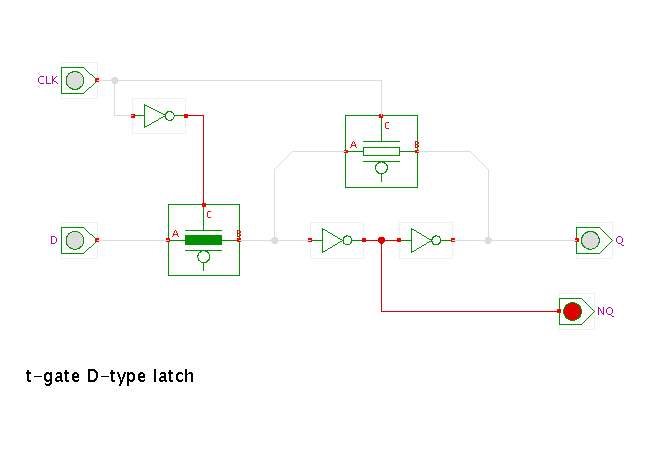
Here, inverters are shown instead of the individual transistors and only the positive control-signal is shown for each transmissiong-gate. As a result, the left-to-right dataflow through the latch when CLK=1 and the feedback loop when CLK=0 should be obvious, literally at a glance.
Click the input switches or type the 'c' and 'd' bindkeys to control the clock and data inputs.
The circuit consists of a t-gate based multiplexer and a non-inverting buffer (built as a cascade of two inverters). One additional inverter is used to generate the inverse of the clock input signal, required to control the transmission-gates. If both the clock signal and the inverted clock signal are available from external circuitry, this inverter can be removed.
The left transmission gate is enabled when the clock input is high, while the right transmission gate is enabled when the clock input is low. Therefore, when the clock input is high, the current value from the data input (D) will propagate through the left transmission gate and through the two inverters. The latch is transparent, and the output value Q follows the data input value, while the NQ output generates the inverse of the data input value.
As soon as the clock signal changes to low (logical 0), the left transmission-gate is switched-off, while the right transmission-gate is activated and becomes conducting. As a result, the output value Q of the flipflop will be fed back into the input of the first-stage inverter. Therefore, the latch stores whatever value it hold when the clock signal changed to low.
Run the applet | Run the editor (via Webstart)